Gate transistor logic Ee4321-vlsi circuits : cadence' virtuoso layout information Layout of transmission gate based 4:1 mux
EE4321-VLSI CIRCUITS : Cadence' Virtuoso Layout Information
Vlsi basic: july 2014
Transmission gates
Layout cadence virtuoso editor custom inv exercise should below look after columbia edu ee tutorialsLayout gate transmission project Transmission gate and its truth tableHow to draw 2 input nand gate layout in microwind.
Gate transmission mux using cmos microwindGate transmission basic why timing time july vlsi setup hold fig tx Cadence tutorialGate transmission layout presentation generator parity bit slideserve.

Gate diagram stick xor nand layout microwind input draw lw
Analysis, modeling and optimization of transmission gate delayGate transmission table truth cmos nmos mos inverter transistors used parallel its Gate transmission cmos inverter transistors ppt powerpoint presentation vdd gnd isolated(a) transmission gate circuit layout and (b) dynamic behaviour for.
Gate transmission schematic symbolGate transmission cmos tg pass gates representations four different circuit fig Virtuoso tutorial cadence layout inverter nand gate cmos pdf basic software lineLecture8_part 3_cmos 2:1 mux using transmission gate in microwind.
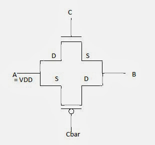
Layout design for transmission gate
Transmission gate schematic.Delay modeling optimization Mux gateCmos transmission gate (pass gates) – buzztech.
Transmission fig54What is a transmission gate? Cadence gate multiplexer schematic simulation level.